- 40033332222
- 819698405@qq.com
- Mon - Fri 9am - 6pm

Manufacturer:: -
Product datasheet: SS-盛世物联关于VOC传感器ENS160的说明书-20201225.pdf
Digital humidity & temperature sensor — specification summary
Digital Metal-Oxide Multi-Gas Sensor
The ENS160 is a digital multi-gas sensor solution, based on metal oxide (MOX) technology with four MOX sensor elements. Each sensor element has independent hotplate control to detect a wide range of gases e.g. volatile organic compounds (VOCs) including ethanol, toluene, as well as hydrogen and nitrogen dioxide with superior selectivity and accuracy. For indoor air quality applications, the ENS160 supports intelligent algorithms to digitally process raw sensor measurements on-chip. These algorithms calculate CO 2 -equivalents, TVOC, various air quality indices (AQIs) and perform humidity and temperature compensation, as well as baseline management – all on chip! Moreover, a development option is available to digitally output raw sensor measurements from each sensor element for customization. The LGA packaged device includes an SPI or I²C slave interface with separate VDDIO to communicate with a main host processor. The ENS160 is a proven and maintenance-free technology, designed for high volume and reliability.
o Cooker hoods o Air cleaners / purifiers
2 Pin Assignment .......................... 5
14.2.2 OPMODE (Address 0x10) ............... 21
3 Absolute Maximum Ratings ............ 6
14.2.3 CONFIG (Address 0x11) ................ 21
4 Electrical Characteristics .............. 7
14.2.4 COMMAND (Address 0x12) ............. 22
5 Air Quality Signal Characteristics .... 8
14.2.5 TEMP_IN (Address 0x13) .............. 23
5.1 TVOC – Total Volatile Organic Compounds .............................. 8
14.2.6 RH_IN (Address 0x15) .................. 23
7 Output Signal Accuracy ............... 11
14.2.9 DATA_ECO2 (Address 0x24) ........... 25
8 Initial Start-Up and Warm-Up ........ 11
14.2.10 DATA_T (Address 0x30) ............... 25
8.1 Initial Start-Up ......................... 11
14.2.11 DATA_RH (Address 0x32) .............. 25
8.2 Warm-Up ................................ 11
14.2.12 DATA_MISR (Address 0x38) ........... 26
9 Recommended Sensor Operation .... 12
14.2.13 GPR_WRITE (Address 0x40) ........... 27
10 Recommended Sensor Storage ....... 12
11.2.2 SPI Timing Information ................ 17
20 Copyrights & Disclaimer .............. 33
The ENS160 digital multi-gas sensor consists of four independent heaters and gas sensor elements, based on metal oxide (MOX) technology and a controller as shown in the functional block diagram below.
Heaters
Sensors
Controller Heater Driver
Sensor Measurement
x 4
INTn
System Control
CSn
Memory
Data Processing
The heater driver controls the sensor operating modes and provides power to the heaters of each individual sensor element. During operation the heater driver regulates the heaters to their individual set-points.
The sensor measurement block determines the value of sensor resistance for each individual sensor element.
The system control block processes the resistance values internally to output calculated TVOC, CO 2 -equivalents and further signals on the digital interface.
The ENS160 includes a standard 2-wire digital I 2 C interface (SCL, SDA) or 4-wire digital SPI interface (SCLK, MOSI, MISO, CSn) for communication to the main host processor.
On-chip memory is used to store calibration values.
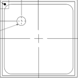
The ENS160 pin assignment is described in the following figures.
Top View Bottom View
Pin 1 Corner
Corner Area
Pins Pin Name Pin Type Description
1 MOSI / SDA Input / Output SPI Master Output Slave Input / I²C Bus Bi-Directional
Data
2 SCLK / SCL Input SPI Serial Clock / I²C Bus Serial Clock Input
3 MISO / ADDR Input / Output SPI Master Input Slave Output / I²C Address Select:
I 2 C ADDR pin high -> 0x53 / ADDR pin low -> 0x52
4 V DD Supply Main Supply Voltage
Also see sections “I 2 C Operation Circuitry” and “SPI Operation Circuitry” for wiring.
See section “Registers” and “DATA_ECO2 (Address 0x24)” on how to obtain equivalent CO 2 - values from the ENS160.
Relative humidity Ethanol reference
Relative Humidity [%]
Concentration [ppm]
ENS160 signal
Extreme humidity conditions (<20% and >80% RH) or sudden, significant changes, thereof may influence the output signals. To overcome such impacts, the ENS160 is equipped with a temperature and humidity compensation algorithm, relying on data from an external temperature and humidity-source, that can be regularly updated to an internal register for processing (See section “Registers” for further information). The diagram on the left shows the ENS160’s response to various ethanol concentrations 1 while impacted by significant humidity changes.
Estimated EtOH conc. [ppb]
Reference ENS160
3 s error 1 s error
Error [%]
The diagrams show the typical and maximum (3σ) accuracies of the ethanol signal. A typical error of maximum 10% of the measured value can be derived.
The ENS160 performance in terms of sensor raw resistance signals and sensitivities will change upon its first power-on. This change in resistance is greatest over the first 48 hours of operation. Therefore, the ENS160 comprises an initial start-up algorithm, allowing its output signals (e.g. eCO 2 and TVOC) to be used from first power-on after 60 minutes of operation in any of the relevant gas sensing modes 2 .
Besides “Initial Start-Up” the conditioning or “Warm-Up” period is the time required to achieve adequate sensor stability before measuring VOCs after long idle periods or power- off. The ENS160 requires a minimum of 5 minutes warm-up before accurate readings can be expected 1 .
For best performance, the sensor shall be operated in normal air with no aggressive or poisonous gases present and the following operating conditions: temperature: -5 to 60°C (typical: 25°C); relative humidity: 20 to 80%RH (typical: 50%RH), non-condensing. Any, particularly prolonged exposure to environments outside these conditions may affect performance and lifetime of the sensor.
The guidelines under “Recommended Sensor Operation” also apply for its storage.
The ENS160 is an I 2 C or SPI Slave device.
If the CSn is held high, the interface behaves as an I²C slave. At power up the condition of the MISO/ADDR pin is used to determine the LSB of the I²C address. The I²C slave address is 0x52 (MISO/ADDR low) or 0x53 (MISO/ADDR high).
If the CSn pin is asserted (low) the interface behaves as an SPI slave. This condition is maintained until the next Power-on Reset.
Both the SPI and I²C slave interfaces use the same register map for communication.
The ENS160 is an I 2 C slave device with a fixed 7-bit address 0x52 if the MISO/ADDR line is held low at power-up or 0x53 if the MISO/ADDR line is held high.
The I 2 C interface supports standard (100kbit/s), fast (400kbit/s), and fast plus (1Mbit/s) mode. Details on I²C protocol is according to I²C-bus specifications [UM10204, I²C-bus specification and user manual, Rev. 6, 4 May 2014].
The device applies all mandatory I²C protocol features for slaves: START, STOP, Acknowledge and 7-bit slave address. None of the other optional features (10-bit slave address, general call, software reset or Device ID) are supported, nor are the master features (Synchronization, Arbitration, START byte).
The Host System, as an I²C master, can directly read or write values to one of the registers by first sending the single byte register address. The ENS160 implements “auto increment” which means that it is possible to read or write multiple bytes (e.g. read multiple DATA_X bytes) in a single transaction.
Standard Fast Fast Mode Plus
Parameter Symbol
Hysteresis of Schmitt trigger inputs V hys - - 0.05xV DDIO - 0.05xV DDIO - V
Input current each I/O pin I i -10 10 -10 10 -10 10 µA
Parameter Symbol Standard Fast Fast Mode Plus Unit Min Max Min Max Min Max
Hold time (repeated) START con- dition. After this period, the first clock pulse is generated
t HD_STA 4 - 0.6 - 0.26 - µs
Set-up time for a repeated START condition t SU_STA 4.7 - 0.6 - 0.26 - µs
Data set-up time t SU_DAT 250 - 100 2 - 50 2 - ns
Data hold-time t HD_DAT 0 3 3.45 4 0 3 0.9 4 0 3 - µs
Set-up time for STOP condition t SU_STO 4.0 - 0.6 - 0.26 - µs
Bus free time between a STOP and START condition t BUF 4.7 - 1.3 - 0.5 - µs
S Sr P S
After the START condition, in the first transaction:
Slave address
Register address
Acknowledge from slave
Data byte
Acknowledge from master
Data byte 1
Data byte n Last data byte
After the START condition, in a single continuous transaction:
Data to register
Master transmitter
The SPI interface is a slave bus that can operate with up to 10MHz clock-frequency.
It shares pins with the I²C interface. SPI is selected and SPI transfer initiated by asserting the CSn line low. Once the CSn line has been asserted low the ENS160 will not accept I²C transactions until the next Power-On Reset.
Data is clocked in on the rising edge of SCLK; most significant bit first.
During a Read operation, data is clocked out on the falling edge of SCLK so it is stable for the following riding edge.
MISO stays in high impedance mode until the device is selected (CSn low). Data on MISO is only valid on a Read operation.
A transaction starts with the target address and R/W control bit in the first byte followed by the read or write data.
In a Read operation Auto-increment of the address enables multiple registers to be read in sequence. CSn de-asserting (to high) terminates the Read sequence.
A Read SPI frame is composed as follows:
In a Write operation, the address does not Auto-increment. Multiple writes can be performed by alternating Address and Data bytes. CSn de-asserting (to high) terminates the Write sequence.
A Write SPI frame is composed as follows:
Please refer to first pages for functional description.
At power-up, the ENS160 configures itself from a reset state and prepares for commands over the serial bus via either I 2 C or SPI Protocols.
The default state is OPMODE 1, which is an IDLE condition that enables ENS160 so that it may respond to several commands. In this mode it is not operating as a gas sensor.
OPMODE 0 is a very low power standby state. ENS160 exits from the standby state when the user asks to execute a different OPMODE.
Active OPMODEs are described further in the OPMODE Register section.
When active gas sensing OPMODEs are running, new data is notified either via the interrupt (INTn) or by polling the DATA_STATUS register. The output of the gas sensing OPMODEs are presented in the DATA_XXX registers which can be read at any time.
Write 0x00
Mode
E.g. COMMAND
Write 0x01
Load of Customer
Sequence
OPMODE Write 0x01
OPMODE Write 0x02-0xFF
Write 0x02-0xFF
Modes
This section describes the registers of the ENS160 which enable the host system to
Note that some registers are actually spread over multiple addresses. For example, PART_ID at address 0 is spread over 2 addresses (its “Size” is 2). Registers are stored in little endian so the LSB of PART_ID is at address 0 and the MSB of PART_ID is at address 1.
This 2-byte register contains the part number in little endian of the ENS160.
The value is available when the ENS160 is initialized after power-up.
Address 0x00 PART_ID
This 1-byte register sets the Operating Mode of the ENS160. The Host System can write a new OPMODE at any time including when the ENS160 is in DEEP SLEEP.
Any current operating mode will terminate and the new operating mode will start.
Address 0x10 OPMODE
7:0 0x00 R/W Operating mode: 0x00: Deep sleep mode (low power standby) 0x01: Idle mode (low-power) 0x02 – 0xFF: Gas Sensing Modes (except 0x0F) 0x0F: Software reset (full system reset)
In Deep sleep mode, ENS160 has limited functionality but will respond to an OPMODE write.
Idle Mode is intended for configuration before running an active sensing mode.
0x02-0xFF (except 0x0F) are active gas sensing operating modes.
This 1-byte register configures the action of the INTn pin which allows the ENS160 to signal to the host system that particular data is available.
The INTn pin can be (de-)asserted (polarity configurable) when ENS160 updates GPR_Read registers, or when it updates DATA registers, or when a certain threshold is reached (set through COMMAND mode).
A typical setting 0x23 would enable an active low interrupt (no pull-up required) when new output data is available in the DATA registers.
Address 0x11 CONFIG
6 INTPOL 0b0 R/W INTn pin polarity: 0: Active low (Default)
5 INT_CFG 0b0 R/W INTn pin drive: 0: Open drain
2 INTTH 0b0 R/W INTn pin asserted when previously configured thresholds are reached
1 INTDAT 0b0 R/W INTn pin asserted when new data is presented in the DATA_XXX Registers
0 INTEN 0b0 R/W INTn pin is enabled for the functions above
This 1-byte register allows some additional commands to be executed on the ENS160. This register can be written at any time, however, commands will only be actioned in IDLE mode (OPMODE 0x01).
The COMMAND register allows multiple interactions with the system where data needs to be passed between the user/host and the ENS160.
Typically, a request for data (e.g. GetVer) will result in the requested data being placed in the General Purpose READ Registers and an input of data (e.g. set alarm threshold) would first be stored in the General Purpose WRITE Registers at address 0x40-47.
Below is a list of valid commands for the ENS160.
Address 0x12 COMMAND
7:0 Command 0x00 R/W List of commands 0x01: GETVER – Get ENS160 Version
After issuing GetVer, the version of the ENS160 will be placed in General Purpose Registers GPR_READ0 and GPR_READ1. The NEWGPR bit in DATA_STATUS will be set and the INTn asserted if configured to react to NEWGPR.
This 2-byte register allows the host system to write ambient temperature data to ENS160 for compensation. The register can be written at any time. TEMP_IN_LSB should be written first as the update is recognized on a write to TEMP_IN_MSB.
Address 0x13 TEMP_IN
The format of the temperature data is the same as the format used in the ENS21x as shown below:
Temperature in Kelvin * 64. Kelvin = Celsius + 273.15. 0x4A8A is equivalent to 25 Celsius.
Byte 0x14 Byte 0x13
This 2-byte register allows the host system to write relative humidity data to ENS160 for compensation. The register can be written at any time. RH_IN_LSB should be written first as the update is recognized on a write to RH_IN_MSB.
Address 0x15 RH_IN
The format of the relative humidity data is the same as the format used in the ENS21x as shown below:
Relative Humidity * 512.
Byte 0x16 Byte 0x15
This 1-byte register indicates the current STATUS of the ENS160.
Address 0x20 DATA_STATUS
6 STATER 0b0 R High indicates that an error is detected. E.g. Invalid Operating Mode has been selected.
5 - 0b0 R Reserved
4 THRESH 0b0 R High means that the threshold (for xxx, if previously set) has been reached.
High indicates that a new data is available in the DATA_x registers. Cleared automatically at first DATA_x read.
High indicates that a new data is available in the GPR_READx registers. Cleared automatically at first GPR_READx read.
During operation, Bit 6 (STATER) of DATA_STATUS is asserted if an error has occurred.
Further information regarding the error can be read from the GPR_READ registers.
The meaning of the errors may be different, depending on the operation being undertaken.
This 2-byte register reports the calculated TVOC concentration in ppb.
Address 0x22 DATA_TVOC
This 2-byte register reports the calculated equivalent CO 2 -concentration in ppm. It is based on the detected VOCs and hydrogen.
Address 0x24 DATA_ECO2
This 2-byte register reports the temperature used in its calculations (taken from TEMP_IN, if supplied).
Address 0x30 DATA_T
The format of the temperature data is the same as the format used in the ENS21x.
Byte 0x30 Byte 0x31
This 2-byte register reports the relative humidity used in its calculations (taken from RH_IN if supplied).
Address 0x32 DATA_RH
Relative Humidity * 512. 0x6400 is equivalent to 50%RH.
Byte 0x32 Byte 0x33
This 1-byte register reports the calculated checksum of the previous DATA_ read transaction (of n-bytes). It can be read as a separate transaction, if required, to check the validity of the previous transaction. The value should be compared with the number calculated by the Host system on the incoming Data.
Address 0x38 DATA_MISR
This 8-byte register is used by several functions for the Host System to pass data to the ENS160.
Writes to these registers are not valid when the ENS160 is in DEEP SLEEP or during a low power portion of an operating mode. Writes should only be done during IDLE mode (OPMODE 0x01).
Address 0x40 GPR_WRITE0-7
This 8-byte register is used by several functions for the ENS160 to pass data to the Host System.
When New GPR_DATA is available the NEW_GPR bit of the DATA_STATUS register will be set and the INTn pin asserted (if configured).
Address 0x48 GPR_READ0-7
1. CSn must be pulled high (directly to V DDIO ) to ensure I 2 C interface is selected
2. MISO/ADDR should be pulled low or high to specify the LSB of the address
3. Pull-up resistors The above recommendation for pull-up resistance values applies to I 2 C standard mode only. Pull-up resistors for SCL and SDA are assumed to be part of the host system and should be selected dependent on the intended I 2 C data rate and individual bus architecture.
The recommended application circuit for the ENS160 for SPI interface is shown below:
SPI_CSn
1. Weak pull-up resistor may be required for MISO to define the level when tri-stated
The ENS160 uses an open LGA package. This package can be soldered using a standard reflow process in accordance with IPC/JEDEC J-STD-020D.
Temperature [°C]
t SOAK t 3
Time [s]
t 2
t 1
The detailed settings for the reflow profile are shown in the table below.
Parameter Reference Rate / Unit
Average temperature gradient in preheating 2.5K/s
Soak temp range
Ts min 150°C
Peak temperature in reflow T PEAK 260°C
Temperature gradient in cooling Max. -5K/s
It is recommended to use a no-clean solder paste. There should not be any board wash processes, to prevent cleaning agents or other liquid materials contacting the sensor area.
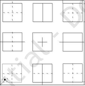
Pin 1 Corner Index Area
(Top View) (Side View)
n X L
n X W
(Bottom View)
Parameter Symbol Dimensions
Top View
1. All dimensions are in millimeters
The package has a marking with TC_4 trace-code according to Cspec 507870020.
| multiple outputs e.g. eCO | , and TVOC | in | Indoor air quality detection |
|---|---|---|---|
| 2 | o |
| compliance with worldwide IAQ | -signal | o Demand-controlled ventilation |
|---|---|---|
| standards | Smart thermostats |
| Key Features & Benefits ......................... 2 | 13 | Operation ............................... 19 | |
|---|---|---|---|
| Applications ....................................... 2 | 14 | Registers ................................ 20 | |
| Properties ......................................... 2 | 14.1 | Register Overview ..................... 20 | |
| Content Guide .................................... 3 | 14.2 | Detailed Register Description ........ 21 | |
| 1 | Block Diagram ........................... 4 | 14.2.1 | PART_ID (Address 0x00) ............... 21 |
| 5.2 | eCO – Equivalent CO | .................. 8 | ||
|---|---|---|---|---|
| 2 | 2 | 14.2.7 | DATA_STATUS (Address 0x20) ........ 24 | |
| 6 | Humidity Compensation .............. 10 |
| 11 | Host Communication .................. 13 | 14.2.14 | GPR_READ (Address 0x48) ............ 27 |
|---|---|---|---|
| 11.1 | I 2 C Specification ....................... 13 | ||
| 15 | Application Information ............... 28 |
| 11.1.1 | I C Description ......................... 13 | 15.1 | I 2 C Operation Circuitry ................ 28 |
|---|---|---|---|
| 11.1.2 | I 2 C I/O and Timing Information ...... 13 | 15.2 | SPI Operation Circuitry ................ 29 |
| 11.1.3 | I 2 C Read Operation .................... 15 | 16 | Soldering Information ................. 30 |
| 17 | Package Drawings & Markings ........ 31 | ||
| 11.1.4 | I 2 C Write Operation ................... 16 | ||
| 18 | Ordering & Contact Information ..... 32 | ||
| 11.2 | SPI Specification ....................... 17 | ||
| 19 | RoHS Compliance & ScioSense Green | ||
| 11.2.1 | SPI Description ......................... 17 |
| 11.2.3 | SPI Read Operation .................... 18 | 21 | Document Status ....................... 34 |
|---|---|---|---|
| 11.2.4 | SPI Write Operation ................... 18 | 22 | Revision Information .................. 34 |
| 12 | Functional Description ................ 18 |
| 5 | V DDIO | Supply | Interface Supply Pins |
|---|---|---|---|
| 6 | INTn | Output | Interrupt to Host |
| 7 | CSn | Input | SPI Interface Select (CSn low -> SPI / CSn high -> I | C) |
|---|---|---|---|---|
| 8, 9 | V | Supply | Ground Supply Voltage |
| 0 | 200 | 400 | 600 | 800 | 1000 | 0 | 200 | 400 | 600 | 800 | 1000 |
|---|---|---|---|---|---|---|---|---|---|---|---|
| Reference EtOH concentration [ppb] | Reference EtOH concentration [ppb] |
| Parameter | Maximum Time | Comment | |
|---|---|---|---|
| Initial Start-Up | 60 minutes | See below for further details | |
| Warm-Up | 5 minutes | See below for further details |
| Min | Max Min Max Min | Max | |
|---|---|---|---|
| Low level input voltage | V -0.5 0.3xV | -0.5 0.3xV -0.5 | 0.3xV V |
| IL | DDIO DDIO | DDIO | |
| High level input voltage | V IH 0.7xV DDIO | 2.39 0.7xV DDIO 2.39 0.7xV | DDIO 2.39 V |
| @ 2mA sink current | OL2 | DDIO DDIO | |||
|---|---|---|---|---|---|
| Low-level output current @ 0.4V | I OL | 3 | 3 | 20 mA | |
| Output fall time from V | IHmin to | 20xV DDIO | / 20xV DDIO / | ||
| t | 250 | 250 250 ns | |||
| V | OF | 5.5 | 5.5 |
| Min | Max | Min | Max | Min | Max | |||
|---|---|---|---|---|---|---|---|---|
| SCLK clock frequency | f | 0 | 100 | 0 | 400 | 0 | 1000 | kHz |
| LOW period of the SCLK clock | t LOW | 4.7 | - | 1.3 | - | 0.5 | - | µs |
|---|---|---|---|---|---|---|---|---|
| HIGH period of the SCLK clock | t | 4.0 | - | 0.6 | - | 0.26 | - | µs |
| Rise time of SDA and SCLK signals | t r | - | 1000 | 20 300 | 20 120 | ns |
|---|---|---|---|---|---|---|
| 20xV | DDIO / | 20xV DDIO / | ||||
| Fall time of SDA and SCLK signals | t | - | 300 | 300 | 120 | ns |
| Capacitive load for each bus line | C b | - | 400 - | 400 | - | 550 | pF |
|---|---|---|---|---|---|---|---|
| Noise margin at the LOW level | V | 0.1xV | - 0.1xV | - | 0.1xV | - | V |
| nL | DDIO | DDIO | DDIO | ||||
| Noise margin at the HIGH level | V | 0.2xV | - 0.2xV | - | 0.2xV | - | V |
| nH | DDIO | DDIO | DDIO |
| t HD_STA | t HD_DAT | t SU_DAT | t SU_STA | t r | BUF | ||
|---|---|---|---|---|---|---|---|
| t | t | t | t | t | |||
| LOW | r | HIGH | f | SP | |||
| t f | t SU_STO |
| All values referred to V | IHmin and V | ILmax levels | |
|---|---|---|---|
| 2 A fast mode I²C bus device can be used in Standard mode I²C bus system, but the requirement t | >= 250ns must then be |
| Acknowledge from slave Acknowledge from master | No acknowledge from master | ||
|---|---|---|---|
| SCLK 1 2 3 | 4 5 6 7 8 9 1 2 3 4 5 6 7 8 9 | 1 2 3 4 5 6 7 | 8 9 S |
| Slave address | Register address | Data to register | Data to register + n | ||
|---|---|---|---|---|---|
| SDA | A AD6 AD5 AD4 AD3 AD2 AD1 AD0 | A | A |
| Parameter | Symbol | Condition | Min | Typ | Max | Unit | |
|---|---|---|---|---|---|---|---|
| SPI Clock (SCLK) Frequency | FSCLK | 10 | MHz | ||||
| CSn falling to MISO Enabled | TEN | 25pF load | 20 | ns | |||
| CSn rising to MISO Disable | TDIS | 25pF load | 20 | ns | |||
| MOSI Setup Time before SCLK | TSUPI | 15 | ns | ||||
| MOSI hold time after rising SCLK | THLDI | 15 | ns | ||||
| CSn low to first rising SCLK | TLEAD | 20 | ns | ||||
| Last SCLK low to CSn high | TLAG | 20 | ns | ||||
| SCLK High Time | TSCLKH | 40 | ns | ||||
| SCLK Low Time | TSCLKL | 40 | ns | ||||
| SCLK falling to MISO Valid | TVALID | 25pF load | 40 | ns |
| MOSI ADDR6 | ADDR5 | ADDR4-1 | ADDR0 | R/W DATA_IN_MSB | DATA_IN DATA_IN_LSB | SEQUENCE | |
|---|---|---|---|---|---|---|---|
| TEN | TVALID | THLDO | TDIS |
| Byte | Bit Name | Description | |
|---|---|---|---|
| 0 | 7:1 AD[6:0] | On MOSI: Address of the register to Read | |
| 0 | 0 RW | On MOSI: 1: bytes are to be read, starting from AD[6:0]. | |
| 1 | 7:0 RDATA[7:0] | Output on MISO; MOSI ignored | |
| n | 7:0 RDATA[7:0] | Output on MISO; MOSI ignored | |
| 11.2.4 | SPI Write Operation |
| Byte Bit | Name | Description | |
|---|---|---|---|
| 0 7:1 | AD[6:0] | On MOSI: Address of the register to Write | |
| 0 0 | RW | On MOSI: 0: bytes are to be Written, at AD[6:0]. | |
| 1 7:0 | WDATA[7:0] | Input on MOSI; MISO Dummy Data | |
| even 7:1 | AD[6:0] | On MOSI: Address of the register to Write | |
| even 0 | RW | On MOSI: 0: bytes are to be Written, at AD[6:0]. | |
| odd 7:0 | WDATA[7:0] | Input on MOSI; MISO Dummy Data | |
| 12 Functional Description |
| Address | Name | Size | Access | Description | ||
|---|---|---|---|---|---|---|
| 0x00 | PART_ID | 2 | Read | Device Identity 0x01, 0x60 | ||
| 0x10 | OPMODE | 1 | Read / Write | Operating Mode | ||
| 0x11 | CONFIG | 1 | Read / Write | Interrupt Pin Configuration | ||
| 0x12 | COMMAND | 1 | Read / Write | Additional System Commands | ||
| 0x13 | TEMP_IN | 2 | Read / Write | Host Ambient Temperature Information | ||
| 0x15 | RH_IN | 2 | Read / Write | Host Relative Humidity Information | ||
| 0x17 – | - | 1 | - | Reserved |
| 0x20 | DEVICE_STATUS | 1 | Read | Operating Mode | |
|---|---|---|---|---|---|
| 0x21 | - | 1 | Read | Reserved | |
| 0x22 | DATA_TVOC | 2 | Read | TVOC Concentration (ppb) | |
| 0x24 | DATA_ECO2 | 2 | Read | Equivalent CO | 2 Concentration (ppm) |
| 0x26 | - | 2 | Read | Reserved | |
| 0x28 | - | 2 | Read | Reserved | |
| 0x2A | - | 2 | Read | Reserved | |
| 0x2C – | - | 1 | - | Reserved |
| 0x30 | DATA_T | 2 | Read | Temperature used in calculations |
|---|---|---|---|---|
| 0x32 | DATA_RH | 2 | Read | Relative Humidity used in calculations |
| 0x34 – | - | 1 | - | Reserved |
| 0x38 | DATA_MISR | 1 | Read | Data Integrity Field (optional) |
|---|---|---|---|---|
| 0x40 | GPR_WRITE[0:7] | 8 | Read/Write | General Purpose Write Registers |
| 0x48 | GPR_READ[0:7] | 8 | Read | General Purpose Read Registers |
| Bits | Field Name | Default | Access | Field Description | |
|---|---|---|---|---|---|
| 0:7 | PART_ID_LSB | 0x60 | read | Lower Byte of Part ID | |
| 8:15 | PART_ID_MSB | 0x01 | read | Upper Byte of Part ID | |
| 14.2.2 | OPMODE (Address 0x10) |
| Bits | Field Name | Default | Access | Field Description | |
|---|---|---|---|---|---|
| 7:0 | 0x00 | R/W | Operating mode: |
| Bits | Field Name | Default | Access | Field Description | |
|---|---|---|---|---|---|
| 7 | - | 0b0 | - | Reserved | |
| 6 | INTPOL | 0b0 | R/W | INTn pin polarity: |
| 4 | - | 0b0 | - | Reserved |
|---|---|---|---|---|
| 3 | INTGPR | 0b0 | R/W | INTn pin asserted when new data is presented in the |
| Bits | Field Name | Default | Access | Field Description | |
|---|---|---|---|---|---|
| 7:0 | Command | 0x00 | R/W | List of commands |
| Register | 7 | 6 | 5 | 4 | 3 | 2 | 1 | 0 |
|---|---|---|---|---|---|---|---|---|
| GPR_READ0 | Release | Version | ||||||
| GPR_READ1 | Sub-Version |
| Bits | Field Name | Default | Access | Field Description |
|---|---|---|---|---|
| 0:7 | TEMP_IN _LSB | 0x00 | R/W | Lower Byte of TEMP_IN |
| 8:15 | TEMP_IN_MSB | 0x00 | R/W | Upper Byte of TEMP_IN |
| 7 | 6 5 4 | 3 | 2 | 1 | 0 | 7 | 6 | 5 | 4 | 3 | 2 | 1 | 0 |
|---|---|---|---|---|---|---|---|---|---|---|---|---|---|
| TEMP_IN Integer Part (Kelvin) | TEMP_IN Fractions | ||||||||||||
| 14.2.6 | RH_IN (Address 0x15) |
| Bits | Field Name | Default | Access | Field Description |
|---|---|---|---|---|
| 0:7 | RH_IN _LSB | 0x00 | R/W | Lower Byte of RH_IN |
| 8:15 | RH_IN_MSB | 0x00 | R/W | Upper Byte of RH_IN |
| 7 | 6 5 | 4 | 3 | 2 | 1 | 0 | 7 | 6 5 | 4 | 3 | 2 | 1 | 0 |
|---|---|---|---|---|---|---|---|---|---|---|---|---|---|
| RH_IN Integer Part (%) | RH_IN Fractions | ||||||||||||
| 14.2.7 | DATA_STATUS (Address 0x20) |
| Bits | Field Name | Default | Access | Field Description | |
|---|---|---|---|---|---|
| 7 | STATAS | 0b0 | - | High indicates that an OPMODE is running |
| 3 | - | 0b0 | R | Reserved |
|---|---|---|---|---|
| 2 | - | 0b0 | R | Reserved |
| Bits | Field Name | Default | Access | Field Description |
|---|---|---|---|---|
| 0:7 | TVOC_LSB | 0x00 | R | Lower Byte of DATA_TVOC |
| 8:15 | TVOC _MSB | 0x00 | R | Upper Byte of DATA_TVOC |
| Bits | Field Name | Default | Access | Field Description |
|---|---|---|---|---|
| 0:7 | ECO2_LSB | 0x00 | R | Lower Byte of DATA_ECO2 |
| 8:15 | ECO2_MSB | 0x00 | R | Upper Byte of DATA_ECO2 |
| 14.2.10 | DATA_T (Address 0x30) |
| Bits | Field Name | Default | Access | Field Description |
|---|---|---|---|---|
| 0:7 | DATA_T _LSB | 0x8A | R | Lower Byte of DATA_T |
| 8:15 | DATA_T _MSB | 0x4A | R | Upper Byte of DATA_T |
| 7 | 6 5 4 | 3 | 2 | 1 | 0 | 7 | 6 | 5 | 4 | 3 | 2 | 1 | 0 |
|---|---|---|---|---|---|---|---|---|---|---|---|---|---|
| TEMP_IN Integer Part (Kelvin) | TEMP_IN Fractions | ||||||||||||
| 14.2.11 | DATA_RH (Address 0x32) |
| Bits | Field Name | Default | Access | Field Description |
|---|---|---|---|---|
| 0:7 | DATA_RH _LSB | 0x00 | R | Lower Byte of DATA_RH |
| 8:15 | DATA_RH_MSB | 0x64 | R | Upper Byte of DATA_RH |
| 7 | 6 5 | 4 | 3 | 2 | 1 | 0 | 7 | 6 5 | 4 | 3 | 2 | 1 | 0 |
|---|---|---|---|---|---|---|---|---|---|---|---|---|---|
| RH_IN Integer Part (%) | RH_IN Fractions | ||||||||||||
| 14.2.12 | DATA_MISR (Address 0x38) |
| Bits | Field Name | Default | Access | Field Description | |
|---|---|---|---|---|---|
| 0:7 | DATA_MISR | 0x00 | R | Calculated checksum of the previous transaction | |
| Example: | C-code to calculate MISR on the received DATA, to compare with DATA_MISR: |
| Address | Bits | Field Name | Default | Access | Field Description | |
|---|---|---|---|---|---|---|
| 0x40 | 0:7 | GPR_WRITE0 | 0x00 | R/W | General Purpose WRITE Register 0 | |
| 0x41 | 0:7 | GPR_WRITE1 | 0x00 | R/W | General Purpose WRITE Register 1 | |
| 0x42 | 0:7 | GPR_WRITE2 | 0x00 | R/W | General Purpose WRITE Register 2 | |
| 0x43 | 0:7 | GPR_WRITE3 | 0x00 | R/W | General Purpose WRITE Register 3 | |
| 0x44 | 0:7 | GPR_WRITE4 | 0x00 | R/W | General Purpose WRITE Register 4 | |
| 0x45 | 0:7 | GPR_WRITE5 | 0x00 | R/W | General Purpose WRITE Register 5 | |
| 0x46 | 0:7 | GPR_WRITE6 | 0x00 | R/W | General Purpose WRITE Register 6 | |
| 0x47 | 0:7 | GPR_WRITE7 | 0x00 | R/W | General Purpose WRITE Register 7 | |
| 14.2.14 | GPR_READ (Address 0x48) |
| Address | Bits | Field Name | Default | Access | Field Description | |
|---|---|---|---|---|---|---|
| 0x48 | 0:7 | GPR_READ0 | 0x00 | R | General Purpose READ Register 0 | |
| 0x49 | 0:7 | GPR_READ1 | 0x00 | R | General Purpose READ Register 1 | |
| 0x50 | 0:7 | GPR_READ2 | 0x00 | R | General Purpose READ Register 2 | |
| 0x51 | 0:7 | GPR_READ3 | 0x00 | R | General Purpose READ Register 3 | |
| 0x52 | 0:7 | GPR_READ4 | 0x00 | R | General Purpose READ Register 4 | |
| 0x53 | 0:7 | GPR_READ5 | 0x00 | R | General Purpose READ Register 5 | |
| 0x54 | 0:7 | GPR_READ6 | 0x00 | R | General Purpose READ Register 6 | |
| 0x55 | 0:7 | GPR_READ7 | 0x00 | R | General Purpose READ Register 7 |
| The recommended application circuit for the ENS160 I | 2 C interface operation is shown below: |
|---|---|
| Figure 14: Recommended Application Circuit (I | 2 C Operation) |
| 4. Decoupling capacitor must be placed close to the V | (Pin 4) and V | (Pin 5) supply |
|---|---|---|
| DD | DDIO |
| 2. Decoupling capacitors must be placed close to the V | (Pin 4) and V | (Pin 5) supply |
|---|---|---|
| DD | DDIO |
| Soak time | t SOAK | 2..3 min |
|---|---|---|
| Ts max | 200°C |
| Time above 217°C (T | 1 ) | t 1 | Max. 60s | |
|---|---|---|---|---|
| Time above 230°C (T | 2 ) | t 2 | Max. 50s | |
| Time above T | PEAK -10°C (T | 3 ) | t | Max. 10s |
| Min | Nominal | Max | ||
|---|---|---|---|---|
| Total thickness | A | - | 0.83 | 0.9 |
| D | 3.0 | BSC |
| E | 3.0 | BSC | ||
|---|---|---|---|---|
| Lead Width | W | 0.65 | 0.7 | 0.75 |
| Lead Length | L | 0.65 | 0.7 | 0.75 |
| Lead Pitch | e | 1.05 | BSC |
| 2. PCB land pattern in | dotted lines |
|---|---|
| 3. Add 0.05mm all around the nominal lead width and length for the PCB land pattern |


Symbol Parameter Min Max Units Comments
Electrical Parameters
V DD Supply Voltage -0.3 1.98 V
I SCR Input Current (latch-up immunity) ± 100 mA AEC-Q100-004
Electrostatic Discharge
Operating and Storage conditions
MSL Moisture Sensitivity Level 1 Unlimited floor lifetime
T BODY Max. Package Body Temperature 260 °C IPC/JEDEC J-STD-020
T STRG Storage Temperature -40 125 °C
RH STRG Storage Relative Humidity 5 95 % Non-condensing
T AMB 1 Operating Ambient Temperature -40 85 °C
RH AMB 1 Operating Ambient Rel. Humidity 5 95 % Non-condensing
L T 2 Product Lifetime 10 Years
Stresses beyond those listed under Absolute Maximum Ratings may cause permanent damage to the device. These are stress ratings only. Functional operation of the device at these or any other conditions beyond those indicated under Electrical Characteristics is not implied. Exposure to absolute maximum rating conditions for extended periods may affect device reliability and lifetime.
Note: Although being able to detect potentially safety-relevant gases, the ENS160 is not designed for use in any safety-critical or life-protecting application.
| V DDIO | I/O Interface Supply | -0.3 | 3.6 | V |
|---|---|---|---|---|
| V | MOSI/SDA, SCLK/SCL | -0.3 | 3.6 | V |
| V IO2 | MISO/ADDR, INTn, CSn | -0.3 | V DDIO +0.3 | V |
|---|---|---|---|---|
| V | Input Ground | -0.3 | 0.3 | V |
| ESD HBM | Electrostatic Discharge HBM | ± 2000 | V | JS-001-2014 |
|---|---|---|---|---|
| ESD | Electrostatic Discharge CDM | ± 750 | V | JS-002-2014 |
The following figure details the electrical characteristics of the ENS160.
V DDIO IO Supply Voltage
I DD Average 1 Supply Current 2
Mode 0 (DeepSleep) 3 10 µA
Mode 2 (4 hotplates)
Mode 3 (pulse1) mA
Mode 4 (pulse2) mA
Mode 3 (pulse1) 1 mA
Mode 4 (pulse2) 1 mA
V IH High-level input voltage
V IL Low-level input voltage
MOSI/SDA, MISO [I OL =5mA]
INTN [I OL =2mA] 0.35xV DDIO V
To satisfy a wide range of individual application requirements, the ENS160 offers a series of (indoor) air quality output signals that are derived from various national and international, as well as de-facto standards. Table 4 provides a summary of such signals, with further description in the following sections.
equivalents
About 5,000 to 10,000 different VOCs exist. They are two to five times more likely to be found indoors than outdoors. Indoor VOCs are various types of hydrocarbons from mainly two sources: bio-effluents, i.e. odors from human respiration, transpiration and metabolism, and building material including furniture. VOCs are known to cause eye irritations, headache, drowsiness or, even dizziness, all summarized under the term SBS 1 . Besides industrial applications, comfort aspects (e.g. temperature), or building protection (humidity), VOCs are the one and only root cause for the need to ventilate. Please refer to our “Air Quality Solutions” brochure for further information on VOCs.
To group and classify VOCs, regional guidelines and industry-preferences define a series of compounds and mixtures as reference. E. g ethanol, toluene, acetone, combinations of representatives of the various groups of VOCs (e.g. ISO16000-29), and more, to mention a few.
The ENS160 supplies calibration to ethanol for best, most balanced TVOC-results.
Concentration [ppm]
Taking advantage of its RMR 1 -technology, today, the ENS160 reverses the proportional correlation of VOCs and CO 2 , by providing a standardized output signal in ppmCO 2 - equivalents from measured VOCs plus hydrogen, thus ad-hering to today’s CO 2 -standards, as the diagram on the left testifies: ENS160-based equivalent CO 2 estimate vs. CO 2 , detected by an NDIR-sensor during two consecutive meeting sessions, interrupted by a lunch-break.
Kitchen
smells
Body
odors
Unpleasant
0min 15min 30min 45min 60min
Output
Comment / Recommendation
eCO 2 / CO 2 Rating
The above table shows a typical classification of (equivalent) CO 2 output levels.
| Symbol | Parameter | Conditions | Min | Typ | Max | Unit |
|---|---|---|---|---|---|---|
| V | Positive supply | 1.71 | 1.8 | 1.98 | V |
| Mode 1 (IDLE) | 2 | 2.5 | mA |
|---|---|---|---|
| Mode 2 | 10 | mA |
| Current | 2 4 | (single hotplate) | (<5ms) | |
|---|---|---|---|---|
| Mode 2 | 85 | mA | ||
| (4 hotplates) | (<5ms) |
| V | High-level | MISO | [I =5mA] | 0.8xV | V | |
|---|---|---|---|---|---|---|
| OH | OH | DDIO |
| INTN [I | OH =2mA] | 0.65xV | DDIO | V | |||
|---|---|---|---|---|---|---|---|
| V | Low-level | MOSI/SDA, MISO | 0.2xV | V |
| Parameter | Range | Resolution | Unit | Comment | ||||
|---|---|---|---|---|---|---|---|---|
| TVOC | 0 - 65’535 | 1 | ppb | For | requirements | outside | these | |
| eCO | 400 - 65’535 | 1 | ppmCO | specified ranges please contact us |
| Due to the proportionality between VOCs and -CO | generated by humans, CO | -values |
|---|---|---|
| 2 | 2 |
| Pettenkofer | in the 19 | century) and the unavailability of suitable VOC measurement |
|---|---|---|
| technology made CO | the surrogate of inhabitant-generated air-pollution in confined living |
| Figure 3: ENS160-based equivalent CO | (eCO | ) vs. NDIR-based CO | during two |
|---|---|---|---|
| 2 | 2 | 2 |
| correlation of VOCs and CO | , by providing a standardized output signal in ppmCO | - |
|---|---|---|
| 2 | 2 |
| equivalent CO | 2 output to an NDIR CO | 2 sensor | 800 |
|---|---|---|---|
| in various typical environments: CO | sensors | ||
| 2 | Concentration [ppm] |
| Table 5: Interpretation of CO | and Equivalent CO | Values |
|---|---|---|
| 2 | 2 |
| >1500 | Bad | Heavily contaminated indoor air / Ventilation required | ||
|---|---|---|---|---|
| 1000 - 1500 | Poor | Contaminated indoor air / Ventilation recommended | ||
| 800 - 1000 | Fair | Optional ventilation | ||
| 600 - 800 | Good | Average | ||
| 400 - 600 | Excellent | Target |
Devices sold by ScioSense B.V. are covered by the warranty and patent indemnification provisions appearing in its General Terms of Trade. ScioSense B.V. makes no warranty, express, statutory, implied, or by description regarding the information set forth herein. ScioSense B.V. reserves the right to change specifications and prices at any time and without notice. Therefore, prior to designing this product into a system, it is necessary to check with ScioSense B.V. for current information. This product is intended for use in commercial applications. Applications requiring extended temperature range, unusual environmental requirements, or high reliability applications, such as military, medical life-support or life- sustaining equipment are specifically not recommended without additional processing by ScioSense B.V. for each application. This product is provided by ScioSense B.V. “AS IS” and any express or implied warranties, including, but not limited to the implied warranties of merchantability and fitness for a particular purpose are disclaimed.
ScioSense B.V. shall not be liable to recipient or any third party for any damages, including but not limited to personal injury, property damage, loss of profits, loss of use, interruption of business or indirect, special, incidental or consequential damages, of any kind, in connection with or arising out of the furnishing, performance or use of the technical data herein. No obligation or liability to recipient or any third party shall arise or flow out of ScioSense B.V. rendering of technical or other services.
Information in this datasheet is based on products in the design, validation or qualification phase of development. The performance and parameters shown in this document are preliminary without any warranty and are subject to change without notice.
Datasheet Production Information in this datasheet is based on products in ramp-up to full production or full production which conform to specifications in accordance with the terms of ScioSense B.V. standard warranty as given in the General Terms of Trade.
Discontinued Information in this datasheet is based on products which conform to specifications in accordance with the terms of ScioSense B.V. standard warranty as given in the General Terms of Trade, but these products have been superseded and should not be used for new designs.
1. Page and figure numbers for the previous version may differ from page and figure numbers in the current revision.
2. Correction of typographical errors is not explicitly mentioned.
| Document | Product | Definition | |
|---|---|---|---|
| Status | Status | ||
| Product | Pre- | Information in this datasheet is based on product ideas in the | |
| Preview | Development | planning phase of development. All specifications are design goals |
| Preliminary | Pre- | Information in this datasheet is based on products in the design, |
|---|---|---|
| Datasheet | Production | validation or qualification phase of development. The |
| Datasheet | Discontinued | Information in this datasheet is based on products which conform |
|---|---|---|
| (Discontinued) | to specifications in accordance with the terms of ScioSense B.V. |
| Revision | Date | Comment | Page | |
|---|---|---|---|---|
| 0.9 | 2019-12-11 | Initial Version |